PWM Concept
Pulse Width Modulation is a popular and very commonway of reducing the average voltage. Simply put, it typically involves setting a Vout to oscillate between 0v and Vcc (or someother fixed voltage) at a fixed period and a fixed Duty Cycle. This of course with enough smoothing can produce a very clean signal but for the most part the oscillation alone will work fine for a lot electronic devices. Common usages of PWM are: controlling the speed of a DC motor, dimming an LED or any application that involves “faking” analog outputs.
PWM Frequency
Depending on your application, you may want a high or low PWM frequency. For the process of dimming an led using PWM, frequency of 1Khzcould potentially be fine if you are dealing with just human vision (cameras may need higher frequencies to produce a similar diming effect). Other process such as Buck and boost converters, you may need higher frequencies to produce usable average voltages.
Duty Cycle:
The duty cycle of PWM signal is typically defined as the On Time over the the total Period time. Or effectively, the percentage of on or the percentage of your original voltage.
Example PWM
Lets say we want a 500 khz clock with a duty cycle of 50% the signal would resemble something like this:
 See how the ontime of 1 us over the total period of 2us equates to the 50% duty cycle.
Now for 500 khz clock with duty cyle of 20%
 And at 500 khz your average voltage produce by the pwm signal should be pretty usable for most applications and would produce 50% of your original Vcc in the first signal, and 20% of your original Vcc for the second signal.
RISC-V Builtin PWM Generation (work in-progress)
Since I just got it working I figured I would write up the process I used to get usable PWM signals from the Hifive1 rev b development board.
Overview of PWM Register.
I will try to go into the Register as much as possible, but I still highlighly recommend that you look through the datasheets at the bottom of the article, some very useful information is present in the various documents.
Regardless, the PWM Generation system consists of 3 different separate PWM instances and each of these instances can support four different PWM pins with independent duty cycles. Keep in mind these 3 different instance can have different PWM frequencies but the actual actual individual outputs cannot have different frequencies. Additionally, each pin on the the Hifive1 board has already had a pwm instance if the pins supports the PWM generation system at all. See the the Resources below to determine which pins correlated to which instance and output. Example: PWM Instance 0 is assigned a frequency of 16 mhz, Output 0, 1, 2, 3 can have any duty cycle assigned to them.
PWM Instances and Addresses

Note that the first PWM instance is the least accurate as it has the lowest resolution of the 3 instances
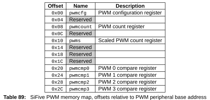
Outline of Memory for Each PWM Instance
 The above Memory map outlines the various locations for each of the revelent registers for each PWM Instance.
General description of PWM generation in the Hifive
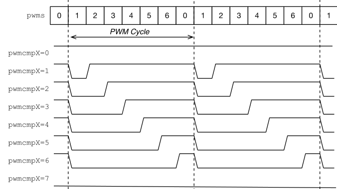
Effectively, how the generation works is that there is a 32 bit counter (pwmcount) that increments based upon a predefined clock. This counter can then be scaled using the pwmcfg register and outputed to the scaled pwm counte register (pwms). This output is then compared to the four compare registers. In the basic not highest accuracy mode of generation, each pwmcmp register (pwmcmp0-3) correspondes to the four outputs of the pwm instance and will raise the output to high when the pwms has exceed some 16 bit or 8 bit value that is stored in a pwmcmp register. The below digram from SiFive makes this concept quite clear.
 Here the diagram assumes our pwms increments from 0 to 6 and shows the various outputs given a set pwmcmp. So if you wanted a 50% duty cycle you would set the pwmcmp to be 3. This method is a bit counter-intuitive as to get 25% duty cycle you have to set pwmcmp to be equal to 6 but this logic can be inverted using some of the GPIO output registers.
PWM Configuration Register
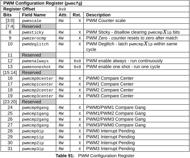
Firstly, I will only be going over the bits in this register that are needed for a simple pwm output, if you wish to do anything more complicated I would recommend you read over the various datasheets that are linked in this article
 Bits [3:0] corresponded to the scaling factor for the pwmcounter to pwmscounter. Keep in mind this takes the input clock and divides i by 2^pwmscale. So if [3:0] = 0010, then your input clock will be divided by 2^2.
Bit 9 is an interesting bit. It allows you to have four first pwm comparator establish period of the signal instead of using the pwms solely. I.e when the pwmcmp0 has value set, and the pwms equals that value or is greater, the pwms, and pwmcounter are reset. At the cost of one less pwm output, there is the possibility of increasing the options of PWM Frequencies. Note you can also just adjust the input frequency for the entire PWM generation instead in order to get a specific frequency but I won’t be describing how to do so in this article. Look in the fe310-manual for information on it
Bit 12 should be set 1 so that the pwm signal is continously generated. Bit 13 is useful if you want to send a signal pulse instead of continuously output the pwm signal. Not needed for a our simple output so leave it to 0. The rest of the bits I won’t go into but they do interesting things like interrupts, centering of the signal, etc. For a simple test the pwmcfg can be assigned 0x00001002 which equates to a pwmscale of 2, and the pwmenalways being set to 1.
PWM Compare Registers.
For each of the compare registers the usable size will be either 16 or 8 bits ( depending on the pwm instance that is used). Effectively, assign the duty cycle to each of these registers but do some minor conversions. In our example for a 50% duty cycle, a value of 0x7FFF will suffice.
GPIO IOF
Since most of the GPIOs have multiple functions beyond being just simple In and Outs, the user has to specifically specify whether or not they want to use one of the addtional functions using the GPIO IOF Registers.

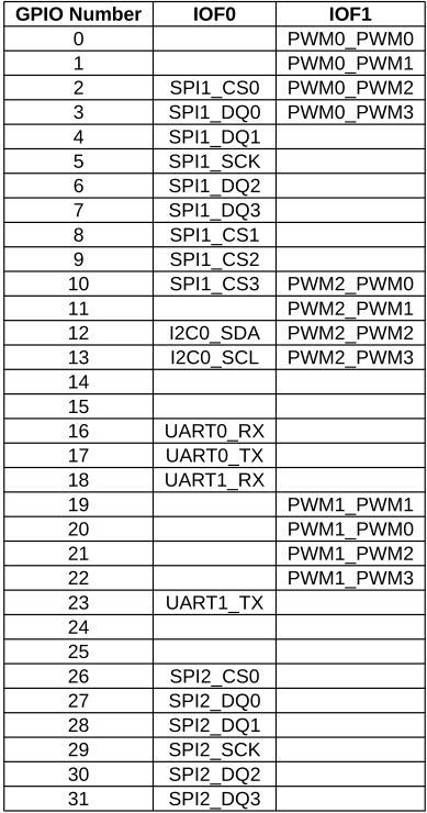
Here the two right columns specify the additional functions that a pin may have assigned to it. To utilize those functions, use these register offsets off of the base GPIO CTRL address 0x038 - for GPIO IOF enable 0x03C - for which iof function
For the purposes of this example, I will be using gpio pin 19, so I effectively have to enable iof and set it to iof1 for that pin:
li t0, 0x10012000 # Base GPIO CTRL Address
li t1, 0x1
SLLI t1, t1, 0x13 # set correct bit to correspond to gpio 19
sw t1, 0x038(t0) # set IOF to be enable for that pin
sw t1, 0x03C(t0) # set IOF select to 1 for second function (i.e pwm function)
Issuing Basic pwm signal:
So combinding everything so far and adding some clears for the important registers:
1
2
3
4
5
6
7
8
9
10
11
12
13
14
15
16
17
18
19
20
21
22
23
24
25
_pwmEn:
	addi sp, sp, -16 # move back store pointer to ad return address to the stack
	sw ra, 12(sp) # store return address to the stack
	li t3, GPIO_LED_ADDR
	li t2, GPIO_CTRL_ADDR
	li t0, PWM1_BASE # Store default ctrl address for pwm0
	li t1, 0x00001002 # Set pwmscale = 2,pwmalways=1
	sw x0, PWMCFG(t0)
	sw x0, PWMCMP0(t0)
	sw x0, PWMCMP1(t0)
	sw x0, PWMCMP2(t0)
	sw x0, PWMCMP3(t0)
	sw x0, PWMSCALE(t0)
	sw x0, PWMCOUNT(t0)
	sw t1, PWMCFG(t0) # Set frequency to roughly 1khz, continously send
	li t1, 0x1FFF # setting duty cycle to 50%
	sw t1, PWMCMP1(t0)
	sw x0, PWMCOUNT(t0)
	sw t3, GPIO_IOF_OFFSET_EN(t2)
	sw t3, GPIO_IOF_OFFSET_SEL(t2)

exit_pwm:
	lw ra, 12(sp)
	addi sp, sp, 16
	ret
Breaking down the above code
Lines 1 and two are just for call purposes (i.e storing ra into the stack for safe keeping). Lines 4,5 are just stardard load for getting the various constants associated with the GPIO. Line 6 is effectively the same as above but for the PWM Instance1 instead of the GPIO Instance. Line 7 is for loading our defined pwm config (pwm always, and pwmscale =2) Lines 8 through 14 are for the precaution of zeroing all critical pwm registers. Line 15 is for actually storing the previously loaded pwm config. Line 16 loads the desired 50% duty cycle into a register. Line 17 stores the duty cycle for our GPIO 19 Line 18 rezeros the pwmcount register just incase it has incremented already. Lines 19 and 20 are for setting the correct IOF settings for GPIO 19
Lines 22 through 25 are just standard exist and return instructions
Alternative PWM Generation
As mentioned above, you can also use the pwmcmp0 for each instance to set the period of the pwm signal at the cost of loosing one pwm output. Also not that you have the to make the appropriate change to the pwmcfg register, (i.e set bit 9 to 1 to enable this functionality) The above code is modified below to support a 50% duty cycle and 0xFFFF written to the pwmcmp0 so that it resets the pwm counter after 0xFFFF counts.
1
2
3
4
5
6
7
8
9
10
11
12
13
14
15
16
17
18
19
20
21
22
23
24
25
26
27
_pwmEn:
	addi sp, sp, -16 # move back store pointer to ad return address to the stack
	sw ra, 12(sp) # store return address to the stack
	li t3, GPIO_LED_ADDR
	li t2, GPIO_CTRL_ADDR
	li t0, PWM1_BASE # Store default ctrl address for pwm0
	li t1, 0x00001202 # Set pwmscale = F, pwmalways=1
	sw x0, PWMCFG(t0)
	sw x0, PWMCMP0(t0)
	sw x0, PWMCMP1(t0)
	sw x0, PWMCMP2(t0)
	sw x0, PWMCMP3(t0)
	sw x0, PWMSCALE(t0)
	sw x0, PWMCOUNT(t0)
	sw t1, PWMCFG(t0) # Set frequency to roughly 1khz, continously send
	li t1, 0xFFFF
	sw t1, PWMCMP0(t0)
	li t1, 0x7FFF # setting duty cycle to 25%
	sw t1, PWMCMP1(t0)
	sw t3, GPIO_IOF_OFFSET_EN(t2)
	sw t3, GPIO_IOF_OFFSET_SEL(t2)
	sw x0, PWMCOUNT(t0)

exit_pwm:
	lw ra, 12(sp)
	addi sp, sp, 16
	ret