Synopsis
This article will be describing some of the repairs that I have performed on the Asrock C2550D4i and C2750D4i. Mostly involving cloning bios chips, bmc chips and some kludges involving pulling clock signals high.
Background
So I have always been semi fond of the Asrock Avoton series of motherboards. They are pretty old as 2021 but they have some decent features (12 sata ports, dual gig ethernet and up to 64GB of memory). All in itx form factor. Unfortunately, these boards have not aged great and have several flaws associated with them.
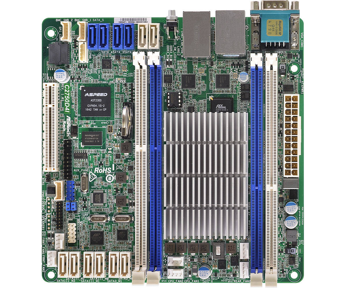
Flaws
- PCICLK Decay
- BMC Chip Decay
- Broadcom Sata Controller Bugs.
PCICLK Decay
This isn’t inheritanly an asrock problem but more of an Intel Atom problem that was associated with the Avoton series where eventually the PCIClk (note this is the clock name on the TPM connector and may be the incorrect term) eventually decays and no longer functions correctly. Note the oscillation does still exist but the average voltage of the clock decays substantially. For example if the a typical 50% 25MHz clock originally had had a Vpp of 3.3V then after a bit eventually decays below the cutoff voltage of on (let’s take 1.8V to be this example cut off voltage). To solve this problem (albeit with a kludge) you can set up a voltage divider with a separte voltage source so that when the original clock signal is high it actually ends up being above the Von threshold. The linked resources below talk about various resistor combinations but I highly recommend you see if you can verify the current Vpp/Vrms of the clock signal before proceeding forward (don’t want to accidently destroy the PCIClk entirely).
Example Clock without Voltage Divider (LTSpice Sim)
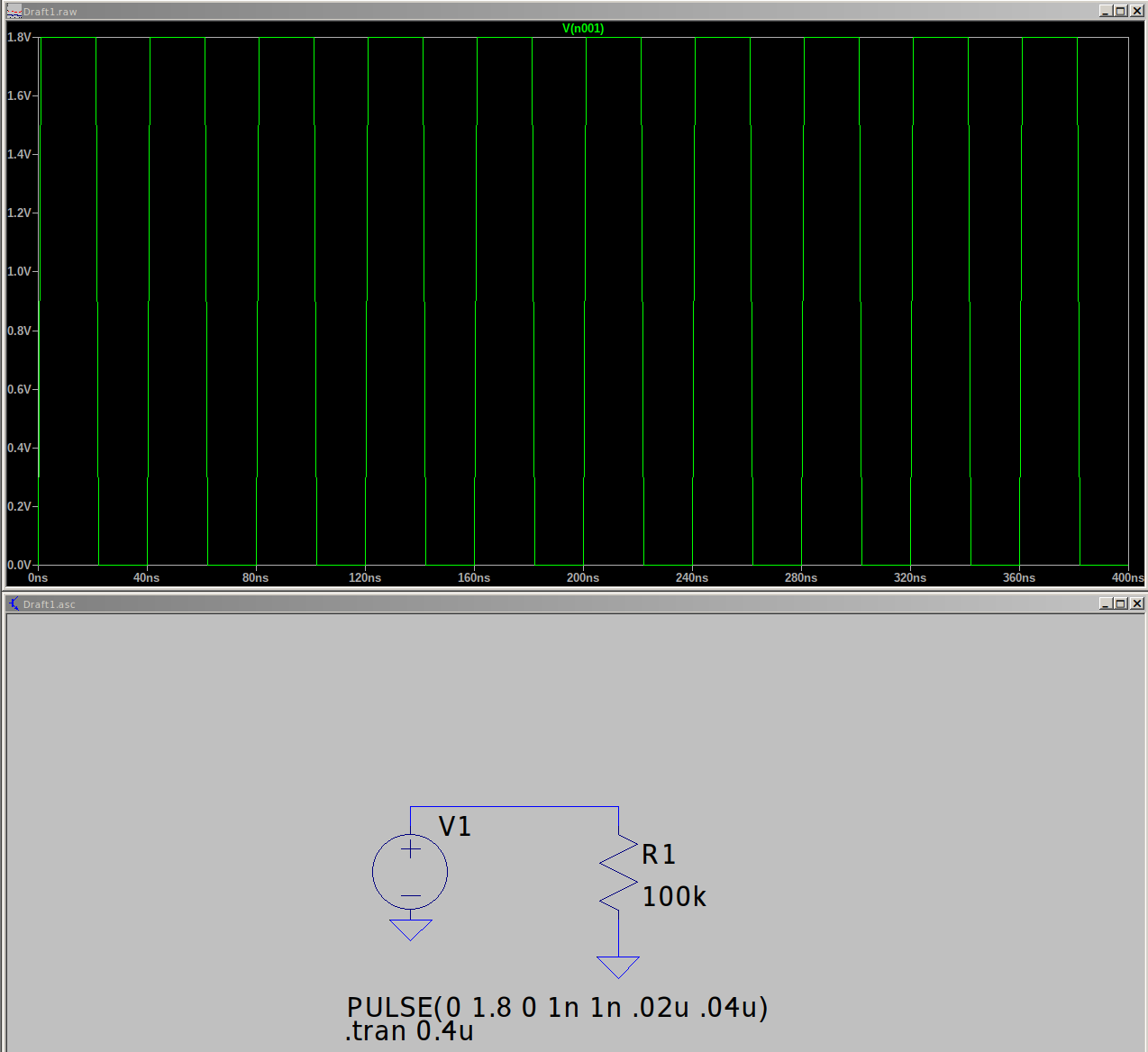 Note the load selection was arbritary, and the clock in this simulation is 25MHz with 10 cycles being displayed.
Example Clock with Voltage Divider Implemented
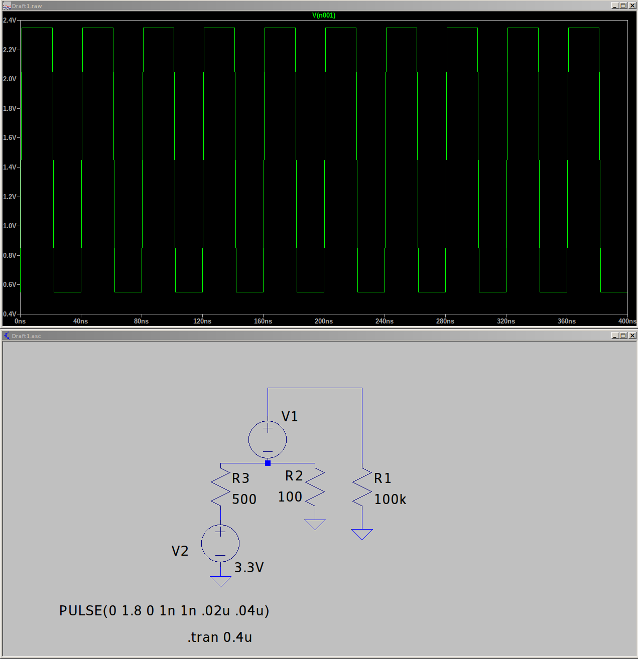 Note the voltage divider in this case adds about .5V which may or may be too much in your case.
##
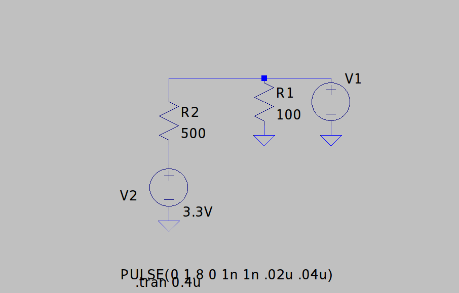
Also note that this above circuit diagram won’t look exactly like that in the actual implementation. The below circuit is closer where V1 is the PCIClk (probably an exposed pin on a header) and the V2 is an arbitrary voltage source.
Broken PCICLK signal without mod
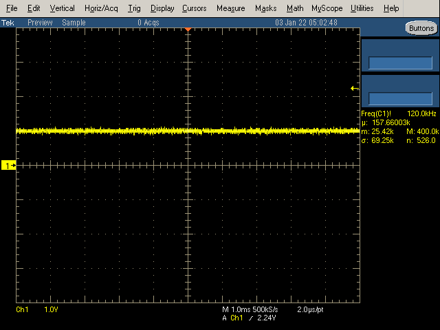
Fixed PCICLK signal without mod
